
Building a High-Side N-MOS Driver for Space Applications
The challenge of high-side switching in space electronics
Switching a load on Earth is simple. Doing it in space, where radiation and temperature extremes can alter every component, is not.
When developing our CubeSat learning platform, we wanted to show how even basic circuits behave under such conditions. Every extra part in orbit increases risk — so our goal was a driver that’s simple, robust, and built with as few radiation-sensitive components as possible.
That’s how our N-MOS driver project began: a 5 V, 1 A high-side switch designed for clarity, cost-efficiency, and real-world teaching value.
The problem we wanted to solve
Most CubeSat systems need to switch power on the high side, between the supply and the load. A P-MOS makes that easy but comes with drawbacks — higher on-resistance, lower radiation tolerance, and higher cost.
We explored using an N-MOS on the high side, which is efficient and widely available, but needs a gate voltage above the supply to turn on fully. Our challenge was to generate that voltage without complex ICs or auxiliary rails — using only discrete, easy-to-understand parts.
Why we chose an N-MOS instead of a P-MOS
P-MOS transistors are convenient but often less efficient and harder to source for space work. N-MOS devices, on the other hand, offer lower losses and better radiation behavior — especially modern GaN FETs, though they’re only available as N-types.
To make an N-MOS act as a high-side switch, its gate must rise above the source. Instead of adding specialized driver chips, we used a charge-pump stage to boost the gate voltage with just a few components.
The charge-pump configuration
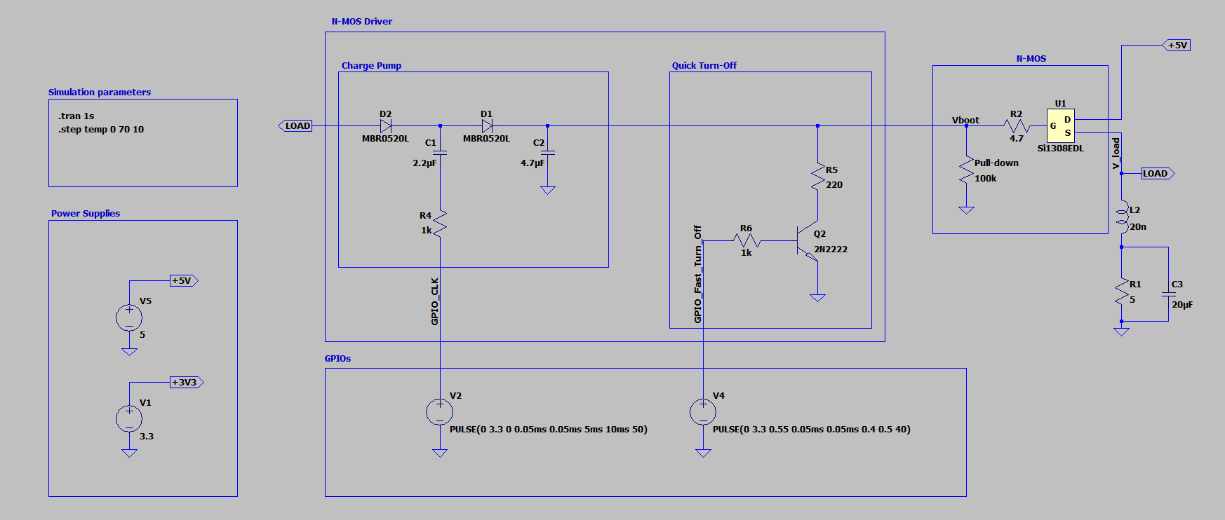
Schematic of the N-MOS high-side driver with charge-pump and fast turn-off stages.
Our design uses a small bootstrap charge pump made of one capacitor, two diodes, and a simple oscillator.
The capacitor charges to 5 V during one phase.
On the next, it lifts the gate potential above the source.
This provides arround 8 V at the gate — enough to fully enhance the N-MOS we choosed (Si1308EDL) and minimize losses. The result is a compact, low-cost driver that’s easy to study and resilient to radiation effects.

LTspice simulation of the N-MOS high-side driver showing the charge-pump operation and fast turn-off response.
Key design decisions
The charge pump provides about 8 V of gate boost, ensuring full enhancement of the N-MOS and low conduction losses while keeping the design compact and efficient.
For controlled power-off, the circuit includes an active fast turn-off stage built around a 2N2222 NPN transistor.
When the control signal drives the 2N2222 into saturation, it creates a low-impedance path between the gate and ground, discharging the gate immediately and turning the MOSFET off — independent of the charge-pump state or system transients.
This approach allows the circuit to cut power instantly in case of anomalies such as a Single-Event Latchup (SEL) or overcurrent event, protecting both the load and the supply.
Designers should account for temperature dependence across the entire circuit. Variations in the 2N2222’s gain and base-emitter voltage, along with changes in the forward drop of the charge-pump diodes, can shift the boosted gate voltage and alter switching timing.
The circuit is therefore temperature-sensitive, and its performance should be verified across the expected thermal range.
Additionally, the threshold voltage (VTH) of the N-MOS will shift with temperature and accumulated Total Ionizing Dose (TID). As radiation increases, V_TH typically drifts upward, reducing gate overdrive and potentially preventing full enhancement. The design must provide enough gate-boost margin to remain operational under those conditions.
The MOSFET used here is intended for teaching and ground testing, but the same architecture can be adapted for space hardware by selecting transistors with characterized TID behavior. GaN FETs remain a promising path forward, combining low losses with strong radiation tolerance.
Pros, cons, and lessons learned
The circuit achieved exactly what we aimed for: a simple, functional high-side N-MOS driver that demonstrates real engineering principles with minimal components.
Pros
Built entirely with discrete, easy-to-source components — ideal for learning and prototyping.
Demonstrates charge-pump gate boosting and fast gate discharge in a transparent way.
Compact, low-cost, and scalable to space use by simply selecting transistors with known radiation data.
Cons
The charge-pump voltage depends on frequency and component tolerances, so it needs validation per application.
Requires two GPIO signals (clock and fast turn-off), which adds some control complexity.
The case of a SEL in the N-MOS still needs to be analyzed.
Overall, the design shows that it’s possible to create space-ready circuits without resorting to expensive or opaque solutions — a core principle in all our Zero2Orbit developments.
Takeaway
This circuit shows that designing for the space sector doesn’t always require complex or expensive ICs. What truly matters is understanding the fundamentals — knowing how each component behaves, how to manage trade-offs, and how to build reliability from simplicity.
By mastering these basics, engineers can lower cost, reduce design errors, and accelerate development, all while keeping their systems ready for the challenges of orbit.
That’s what defines the New Space mindset, and what we aim to share through every Zero2Orbit design: bringing real space engineering closer to everyone.